Reverse-Engineering the LCD Display Interface of the Nest 2nd Gen Thermostat
In which I pried open the glass LCD lens at the front of my Nest 2nd Gen thermostat and found the LCD display module, packaged with a flexible ribbon cable and a round pixel array, and took a months-long journey of reverse engineering, detective work, and problem-solving that taught me more about display interfaces than any tutorial ever could have.
Discovery: Finding the Details of the Display
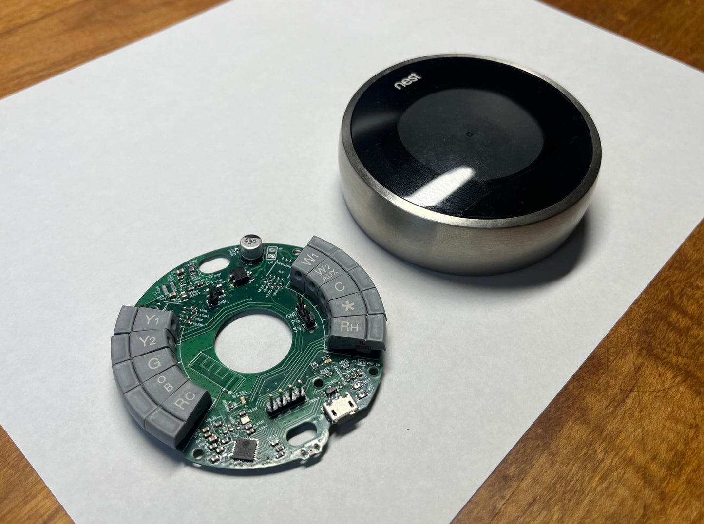
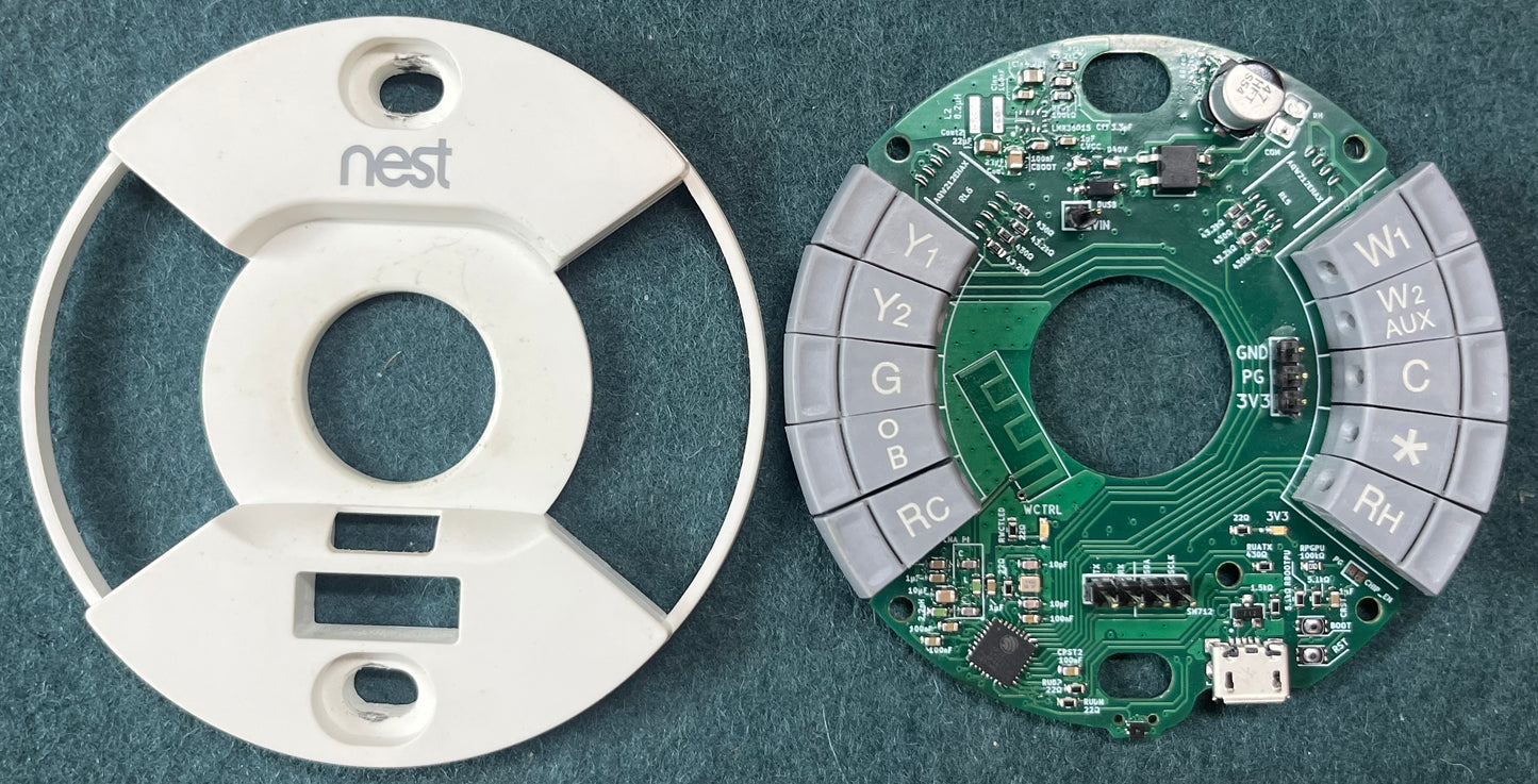
It all started with a disassembled Nest thermostat sitting on my workbench. Following the teardown guide from iFixit, I had carefully disassembled the thermostat until I reached Step 12, where the LCD module was exposed. This is the only step in disassembly that requires prying off glue instead of a screw or a connector.

[Image: iFixit guide showing step 12; Nest thermostat partially disassembled, showing the LCD sandwiched between the front glass and plastic frame]
This revealed a sealed LCD module, with a flexible FPC connector sticking out the side. The display itself is round, although the module is a square with trapezoidal corners.

To get more detail about the module itself, I had to resort to separating the metal frame and peeling back the adhesive layers, and printed in tiny text on the back of the display module: "TM025ZDZ02 FPC1-00 2012-03". A part number! This was my first real clue to start the reverse-engineering adventure.

[Image: Close-up of the back of the LCD module showing the printed part number "TM025ZDZ02"]
The Hunt for Documentation
Armed with a part number, I did what any engineer does: I started hunting for a datasheet. The TM025ZDZ02 proved elusive—it seemed to be a custom or limited-production display. However, I discovered that Shanghai Tianma Micro-Electronics made a very similar module: the TM025ZDZ01. The specifications were nearly identical: a 2.48" round display with 320×320 resolution and a 3-wire SPI interface. You can find them at https://youritech-online.com/products/tm025zdz01-2-48-inch-320x320-tft-lcd-color-screen-circular-display-for-industrial-control-vehicle-handheld-terminal
I managed to obtain the datasheet for the TM025ZDZ01, which had the pinout, the electrical specifications but also code samples for the interface requirements and initialization sequences.
The displays have 320 x 320px square addressable pixels, but only the circular portion is displayed - that is to say you can draw pixels as though they were there in the lower corner, past the radius of the circle, but nothing gets drawn.

Designing the Breakout Board
The datasheet revealed that the display used a 41-pin flexible printed circuit (FPC) connector with a 0.3mm pitch—impossible to work with directly on a breadboard. I needed to create a breakout board to convert these tiny contacts into something manageable.
Using the pinout information from the datasheet, I designed a simple PCB that would break out the FPC connector to standard 2.54mm pins. The board was straightforward—just traces connecting each FPC pin to a corresponding through-hole pad, with clear labeling for each signal.
I was able to buy the FPC connector from DigiKey as Hirose CONN FPC BOTTOM 41POS 0.3MM FH26W-41S-0.3SHW(60) 41 Position FPC Connector Contacts, Bottom 0.012" (0.30mm) Surface Mount, Right Angle and had the PCB manufactured by JLCPCB (#notsponsored).
 [Image: 3D render of the green breakout PCB showing the FPC connector footprint and the arranged pins]
 [Image: From the datasheet, a standard 41-pin FPC connector]
The Interface Challenge: 3-Wire SPI
I could then wire up the display to a breadboard and a microcontroller, but the datasheet specified a "3-wire 9-bit SPI" interface, which immediately raised red flags. Standard SPI is 4-wire (MOSI, MISO, SCLK, CS) and transfers 8-bit bytes. This display was different—it used only 3 wires (SDA, SCL, CS) and required 9-bit transfers.
In a 3-wire SPI protocol, the data line is bidirectional, serving as both MOSI and MISO depending on the direction of communication. The initial bit, the MSB 9th bit in each transfer, indicates whether the byte is a command (0) or data (1)—essentially replacing the dedicated Data/Command pin found in some 4-wire interfaces.

[Image: Timing diagram showing the 3-wire SPI protocol with 9-bit frames]
This created two immediate problems:
- Bus contention: How do you prevent the microcontroller's MOSI from fighting with the display's MISO on the shared data line?
- 9-bit transfers: How do you send 9-bit frames when most SPI hardware natively supports 8-bit transfers?
Solving Bus Contention
The first problem had an easy solution: a simple current-limiting resistor. By placing a resistor (typically 1-2kΩ) in series with the MOSI line, I could prevent bus contention. When the display needed to send data back, the MOSI line can drive the common SDA pin low more strongly than the microcontroller's MOSI output through the resistor can pull it high.

[Image: Simple schematic showing the resistor placement between MCU MOSI and the shared SDA line]
The 9-Bit Protocol: Getting Initial Display Working
Next was reading through the strange commented code in the datasheet to see how I could get the display up and running. I knew that the module used the Driving IC of "S6D05A1" based on the datasheet. So it was off to blend a few sources together:
- The obscure pseudocode in the datasheet of the TM025ZDZ01
- The documentation of the 3-wire SPI protocol
- The detailed documentation of the Color TFT LCD commands in the Samsung S6D05A1's own datasheet.
Using the Toit programming language, the --command and --keep-cs-active flags helped make sure we were sending a 9-bit SPI command as they add in the additional clock tick automatically.
From the breakout board, I hooked up an ESP32C6 SuperMini module, following its hardware SPI GPIO pins:
- Reset: ESP32 pin 15 to pin 3 on the LCD breakout
- MOSI: ESP32 pin 7 to the 1K resistor to SDA (pin 35)
- MISO: ESP32 pin 2 to the 1K resistor to SDA
- CS: ESP32 pin 18 to LCD 34
- CLK: ESP32 pin 6 to LCD 37
Note that the SDI / SDO lines aren't accurately marked because we are using 3-wire, 9-bit SPI instead of 4-wire. This was a really frustrating part of the reverse engineering, because the S6D05A1 also has a mode where it can operate in 4-wire mode, but the 2 datasheets don't have consistent naming across different pages of SDI vs SDO vs SDA.

So in Toit we set up basic commands for read and command of our special 9-bit SPI commands:
import gpio
import spi
MICROSECOND := Duration --us=1

reset := gpio.Pin 15 --output --value=1

clk := gpio.Pin 6 --output --value=0
tx := gpio.Pin 7 --output --value=1 //MOSI
cs := gpio.Pin 18 --output --value=1
rx := gpio.Pin 2 --input --value=1 //MISO


bus := spi.Bus --clock=clk --mosi=tx --miso=rx
device := bus.device --cs=cs --command-bits=1 --frequency=2_000_000

read-spi cmd/int length/int -> ByteArray:
  device.with-reserved-bus:
    print "\nCMD: $(%02x cmd)"
    device.transfer --command=0 #[cmd] --keep-cs-active=true
    data := ByteArray length --initial=0xFF
    device.transfer data --command=1 --read=true
    print data
    return data
  return #[0xFF]


command-spi cmd/int params/ByteArray -> none:
  device.with-reserved-bus:
    device.transfer --command=0 #[cmd]
    params.do: | param | device.transfer --command=1 #[param]
and in hardware, we connected the display breakout to the 9 required pins:

- Pin 1: LED anode to a boost converter at 12.5V
- Pin 2: LED cathode to ground
- Pin 8, 21, 38: GND
- Pin 40, 41: VCC of 3.3V
- Pin 34: SPI Chip Select
- Pin 35: SPI SDA (MOSI/MISO)
- Pin 37: SPI Clock

Following the display setup code from the datasheet, we arrived at this Toit sample program.
Two of the most important lines for our test are to
//Command#[0x2A] //Set_clumn_address to 319, start at the beginning of the display
 command-spi 0x2A #[0x00, 0x00, 0x01, 0x3F]

//Command#[0x2B]//Set_page_address to 319, start at the beginning of the display
  command-spi 0x2B #[0x00, 0x00, 0x01, 0x3F]
the 0x2A and 0x2B commands are how we are going to tell the display what rectangles to write to when we are drawing smaller areas of the screen.
But a lot more goes on for the initial data sequence - for example, we issue all these commands in sequence just to get the display in the mode where we are ready to send it some pixels:
- Toggle the hardware reset pin
- 0x01 // Software Reset
- Read some data to verify that the LCD is responding
- read-spi 0x09 4
- read-spi 0x0A 1
- read-spi 0xA1 4
- 0xF0 // Password 0
- 0xF1 // Password 1
- 0xF2 // 5.2.13. DISCTL // Controls # of scanlines for this display
- 0xF4 // PWRCTL register, sets power and voltage levels
- 0xF5 // VCMCTL (VCOM Control), sets more power and voltage levels
- 0xF6 // SRCCTL (Source Control)
- // Here we could otherwise set the interface mode to 101 - 3-wire 9-bit data Serial interface & RGB Interface IM[3:0]
- // (RIM needs to be 0 for RGB interface mode with 1 transfer per pixel)
- 0xF7 // IFCTL (Interface Control)
- getting the display running on its internal pixel clock vs relying on us to provide dotclocks
- 0xF8 // PANELCTL (Panel Control)
- 0xF9 // GAMMASEL#[Gamma Selection]
- 0xFA // Gamma positive
- 0xFB // Gamma negative
- 0x3A // Interface Pixel Format: 24 bit color vs 16 bit color; set to 24 bit mode 0x77 / "111"= 24-bits/pixel
- 0x11 // Sleep Out
- 0x38 // idle off mode
- 0x29 // Display On
- 0x44 // Tear Scan Line (44h)
- 0x36 // Memory Data Access Control; Set_address_mode
- 0x2A // Set_column_address to 319, start at the beginning of the display
- 0x2B // Set_page_address to 319, start at the beginning of the display
See the full details of the initialization commands here:
main: //Toggle the reset pin reset.set 0 sleep --ms=50 reset.set 1 sleep --ms=120 //Command#[0x01] //Delay#[50]//100ms command-spi 0x01 #[] sleep --ms=100 //Then immediately read some data from the display to make sure the SPI connection works read-spi 0x09 4 read-spi 0x0A 1 read-spi 0xA1 4 // Send the "passwords" of 0x5A to allow further commands to the display //Command#[0xF0] //#[0x5A] //#[0x5A] command-spi 0xF0 #[0x5A, 0x5A] //Command#[0xF1] //#[0x5A] //#[0x5A] command-spi 0xF1 #[0x5A, 0x5A] sleep --ms=30 // WriteCommand(0xF2); 5.2.13. DISCTL (F2h) // 0xF2 // // 0x27 //G1~G320 NL[5:0] 320 scan lines. 3b=480; 0x1d = 240; each bit increment is 8 more scanlines // 0x30 //"NHW[6:0] 5.2.13.2. NHW[7:0]/PIHW[7:0] : Set the horizontal clock (CL1) period in the Normal mode, Partial mode, Idle mode / Partial-Idle mode, respectively. Inhe case of MPU interface mode.default is 64 (0x40)" // 0x03 //PIINV IINV PINV NINV // 0x08 //NVBP[7:0] // 0x08 //NVFP[7:0] // 0x08 //- - - - - - - - - // 0x08 //- - - - - - - - - // 0x00 //- - - - - - - - - // 0x08 //- - - - - - - - - // 0x08 //- - - - - - - - - // 0x00 //- - - - - - - - - // 0x01 //- - - - - SM GS REVerse - for a Normally White LCD // 0x00 //- - - - - - - - // 0x00 //- - - - - - - - // 0x54 //"PIHW[7:0] : Set the horizontal clock (CL1) period in the Partial-Idle mode. In the case of MPU interface mode. default is 64 (0x40) // 0x08 //PIVBP[7:0] // 0x08 //PIVFP[7:0] // 0x08 //RGB_NVBP[7:0] // 0x08 //RGB_NVFP[7:0] command-spi 0xF2 #[0x27, 0x30, 0x03, 0x08, 0x08, 0x08, 0x08, 0x00, 0x08, 0x08, 0x00, 0x01, 0x00, 0x00, 0x54, 0x08, 0x08, 0x08, 0x08] // WriteCommand(0xF4); // PWRCTL register //Command#[0xF4] //#[0x08] //#[0x00] //#[0x00] //#[0x00] //#[0x00] //#[0x00] //#[0x00] //#[0x00] //#[0x00] //#[0x66] //52 GVDD=4.5V/ AVDD=2VCI1 //#[0x02] //VGH=15V,VGL=-7.5V //#[0x00] //#[0x52] //#[0x02] command-spi 0xF4 #[0x08, 0x00, 0x00, 0x00, 0x00, 0x00, 0x00, 0x00, 0x00, 0x00, 0x66, 0x02, 0x00, 0x52, 0x02] // WriteCommand(0xF5); VCMCTL (VCOM Control) //Command#[0xF5] //0xF5 // //0x00 // //0x5C // NVCMH5 Set the VCOMH voltage (a high level voltage at the Vcom alternating drive), It allows ranging from 2.46V to 5.00V //0x5D // VCOM=5.4V 51 // NVML Set the Amplitude of the VCOM voltage on Normal Mode. VCOML is adjusted automatically by setting the Amplitude of VCOM voltage. //0x00 // //0x00 // //0x04 // //0x00 // //0x00 // //0x04 // //0x00 // //0x2A // PIVCMH Set the VCOMH voltage (a high level voltage at the Vcom alternating drive), It allows ranging from 2.46V to 5.00V. PIVCMH[6:0] : Set the amplifying factor of the VCOMH voltage on partial idle mode. //0x21 // PIVML Set the Amplitude of the VCOM voltage on partial idle mode. command-spi 0xF5 #[0x00, 0x5C, 0x5D, 0x00, 0x00, 0x04, 0x00, 0x00, 0x04, 0x00, 0x2A, 0x21] // WriteCommand(0xF6);//SRCCTL (Source Control) //Command#[0xF6]//SRCCTL #[Source Control] //0xF6 // SRCCTL (Source Control) //0x01 // - - - - - SVCIR[2] SVCIR[1] SVCIR[0] //0x00 // - - - SEL_360 - - - SG //0x08 // - - - - SAP[3] SAP[2] SAP[1] SAP[0] //0x03 // - - - - - - OCM[1] OCM[0] //0x01 // - - - - - NSDT[2] NSDT[1] NSDT[0] //0x01 // - - - - NSR_BLK[1]NSR_BLK[0]SR_ND //0x01 // - - - - PISDT[2] PISDT[1] PISDT[0] //0x00 // - - - - PISR_BLK[1] PISR_BLK[0]- - //0x00 // - - command-spi 0xF6 #[0x01, 0x00, 0x08, 0x03, 0x01, 0x01, 0x01, 0x00, 0x00] // We would set the interface mode to 101 - 3-wire 9-bit data Serial interface& RGB Interface IM[3:0] // RIM needs to be 0 for RGB interface mode with 1 transfer per pixel // WriteCommand(0xF7);//IFCTL (Interface Control) //Command#[0xF7]//IFCTL #[Interface Control] //0xF7 // IFCTL (Interface Control) //0x48 // MY_EOR MX_EOR MV_EOR ML_EOR BGR_EOR - - - (BGR EOR = 1, MX_EOR=1) //0x81 // IPM[2:0] default = 100 //MDT[1] MDT[0]SELF_REF DM[1] DM[0] RGB interface mode, MIPI video mode. Not sure we want that? // IPM2 is true. SELF_REF: 0 is External RBG. 1 is self-refresh from internal oscillator. //0x30 // VPL HPL DPL EPL ENDIAN - TE_MON RIM default epl=1. switched vdotclock polarity to falling //0x02 // SPR_SEL - RGB_DIV[2] RGB_DIV[1] RGB_DIV[0] //0x00 // - - - SDO_EN // command-spi 0xF7 #[0x48, 0x81, 0x30, 0x02, 0x00] //CHANGING FFROM 0x81 to 0x80 to get the DISPLAY RUNNING ON ITS INTERNAL OSCILLATOR // ;//RGB_MCU(DM) // command-spi 0xF7 #[0x00, 0x81, 0x30, 0x02, 0x00] //84, 10 for the SPI only mode command-spi 0xF7 #[0x00, 0x84, 0x10, 0x02, 0x00] //84, 10 for the SPI only mode //if we switched to 0x81 default instead of 0x84 we would have DM[1:0] = 01 instead of 00. // DM 0:1 is RGB interface mode control bits sleep --ms=30 // WriteCommand(0xF8);//PANELCTL (Panel Control) //Command#[0xF8]//PANELCTL #[Panel Control] //#[0x11] //default //#[0x00]//default command-spi 0xF8 #[0x11, 0x00] //Command#[0xF9]//GAMMASEL#[Gamma Selection] //#[0x17] command-spi 0xF9 #[0x17] //Command#[0xFA]//Gamma positive 3 //#[0x00]//- - RFP5 RFP4 RFP5 RFP2 RFP1 RFP0 //#[0x02]//- - OSP5 OSP4 OSP3 OSP2 OSP1 OSP0 //#[0x00]//- - PKP05 PKP04 PKP03 PKP02 PKP01 PKP00 //#[0x21]//- - PKP15 PKP14 PKP13 PKP12 PKP11 PKP10 //#[0x2A]//- - PKP25 PKP24 PKP23 PKP22 PKP21 PKP20 //#[0x2D]//- - PKP35 PKP34 PKP33 PKP32 PKP31 PKP30 //#[0x2E]//- - PKP45 PKP44 PKP43 PKP42 PKP41 PKP40 //#[0x22]//- - PKP55 PKP54 PKP53 PKP52 PKP51 PKP50 //#[0x28]//- - PKP65 PKP64 PKP63 PKP62 PKP61 PKP60 //#[0x2F]//- - PKP75 PKP74 PKP73 PKP72 PKP71 PKP70 //#[0x3C]//- - PKP85 PKP84 PKP83 PKP82 PKP81 PKP80 //#[0x3F]//- - PKP95 PKP94 PKP93 PKP92 PKP91 PKP90 //#[0x34]//- - PKP105 PKP104 PKP103 PKP102 PKP101 PKP100 //#[0x00]//- - - - - - - - //#[0x00]//- - - - - - - - //#[0x00]//- - - - - - GLP1 GLP0 command-spi 0xFA #[0x00, 0x02, 0x00, 0x21, 0x2A, 0x2D, 0x2E, 0x22, 0x28, 0x2F, 0x3C, 0x3F, 0x34, 0x00, 0x00, 0x00] //Command#[0xFB]//Gamma negative //#[0x00]//- - RFN5 RFN4 RFN3 RFN2 RFN1 RFN0 //#[0x02]//- - OSN5 OSN4 OSN3 OSN2 OSN1 OSN0 //#[0x34]//- - PKN05 PKN04 PKN03 PKN02 PKN01 PKN00 //#[0x3F]//- - PKN15 PKN14 PKN13 PKN12 PKN11 PKN10 //#[0x3C]//- - PKN25 PKN24 PKN23 PKN22 PKN21 PKN20 //#[0x2F]//- - PKN35 PKN34 PKN33 PKN32 PKN31 PKN30 //#[0x28]//- - PKN45 PKN44 PKN43 PKN42 PKN41 PKN40 //#[0x22]//- - PKN55 PKN54 PKN53 PKN52 PKN51 PKN50 //#[0x2E]//- - PKN65 PKN64 PKN63 PKN62 PKN61 PKN60 //#[0x2D]//- - PKN75 PKN74 PKN73 PKN72 PKN71 PKN70 //#[0x2A]//- - PKN85 PKN84 PKN83 PKN82 PKN81 PKN80 //#[0x21]//- - PKN95 PKN94 PKN93 PKN92 PKN91 PKN90 //#[0x00]//- - PKN105 PKN104 PKN103 PKN102 PKN101 PKN100 //#[0x00]//- - - - - - - - //#[0x00]//- - - - - - - - //#[0x00]//- - - - - - GLN1 GLN0 command-spi 0xFB #[0x00, 0x02, 0x34, 0x3F, 0x3C, 0x2F, 0x28, 0x22, 0x2E, 0x2D, 0x2A, 0x21, 0x00, 0x00, 0x00, 0x00] // 5.1.31. Interface Pixel Format (3Ah) // set to 24 bit mode 0x77 / "111"= 24-bits/pixel //Command#[0x3A] //#[0x77] // command-spi 0x3A #[0x77] //24 bit color command-spi 0x3A #[0x55] //16 bit color // SLEEPOUT R11H //Command#[0x11] //Delay#[120]//120ms command-spi 0x11 #[] sleep --ms=120 //idle off mode //Command#[0x38] command-spi 0x38 #[] // DIPLAYON //Command#[0x29] command-spi 0x29 #[] read-spi 0x09 4 read-spi 0x0A 1 read-spi 0xA1 4 read-spi 0x30 4 // from https://electronics.stackexchange.com/questions/374738/debugging-initialization-of-lcd-with-s6d05a1-driver // LCDWriteCommand(0x44); Tear Scan Line (44h) // LCDWriteData(0x00); // LCDWriteData(0x01); command-spi 0x44 #[0x00, 0x01] //Command#[0x2A] //Set_clumn_address to 319, start at the beginning of the display //#[0x00]//"SC15 SC14 SC13 SC12 SC11 SC10 SC9 SC8" //#[0x00]//"SC7 SC6 SC5 SC4 SC3 SC2 SC1 SC0" //#[0x01]//"EC15 EC14 EC13 EC12 EC11 EC10 EC9 EC8" //#[0x3F]//"EC7 EC6 EC5 EC4 EC3 EC2 EC1 EC0" command-spi 0x2A #[0x00, 0x00, 0x01, 0x3F] //Command#[0x2B]//Set_page_address to 319, start at the beginning of the display //#[0x00]//"SP15 SP14 SP13 SP12 SP11 SP10 SP9 SP8" //#[0x00]//"SP7 SP6 SP5 SP4 SP3 SP2 SP1 SP0" //#[0x01]//"EP15 EP14 EP13 EP12 EP11 EP10 EP9 EP8" //#[0x3F]//"EP7 EP6 EP5 EP4 EP3 EP2 EP1 EP0" command-spi 0x2B #[0x00, 0x00, 0x01, 0x3F]// //Invert colors command, if desired // device.transfer --command=0 #[0x21] // sleep --ms=1000
  // LCDWriteCommand(0x36); //Memory Data Access Control
  // LCDWriteData(0x00);
  command-spi 0x36 #[0x60]


  start:= Time.monotonic-us
  // LCDWriteCommand(0x2C);//Write GRAM

  //HERE'S WHERE WE CAN SET SOME PIXELS

  end := Time.monotonic-us
  print "Duration: $((end - start) / 1_000) ms"

  sleep --ms=5000

The 9-Bit Protocol: Performance Challenges
The performance of the 9-bit transfer requirement was trickier. Most microcontrollers appear to be set up to send ByteArrays, over SPI and the ESP32 is no exception. Sending 9 bits at a time is a weird amount of data compared to the usual 8 bits.
SPI is a serial bus, which means we are sending one bit at a time. So then at 6.2MHz, with a 320 * 320 display, 9 bits per command, and 2 bytes of color data per pixel (in 16 bit color), then 320 * 320 * 9 * 2 / 6200000 = 0.293s is the theoretical maximum speed for drawing a full frame, assuming we clock a bit every chance we get and there's no overhead for the microcontroller. That's nearly 300ms which is 3x the refresh rate that humans can perceive as lag (100ms).
While the TM025ZDZ01 supports a 24-bit parallel bus, managing all the extra hardware seemed like a big step up in complexity. I was wondering if I could get acceptable drawing performance with SPI only.
Per the datasheet, the display's SPI bus will operate at a maximum of 15.15 MHz - which would be 121ms to draw a whole frame. That's pretty close to the human lag perception target.

So a few other things we'd need to get working for a useful display:
- Need to be able to clock much faster than 6.2MHz. Ideally up around 12-15MHz.
- Need to be able to draw small areas of the screen, because we can't afford to freshly draw the entire screen (See earlier comments about the 0x2A and 0x2B commands)
Helpfully, it seems like a lot of these color LCDs follow a similar command structure and the Toit Color-TFT library as well as the LVGL project have been instructive in making sure we have a performant LCD driver.
Powering the Backlight
The final piece of the puzzle was the backlight. The display module included four white LEDs that required a higher voltage than my 3.3V microcontroller could provide. The datasheet specified that each LED had a forward voltage of about 3.2V and needed 20mA of current.
I solved this with an adjustable boost converter based on the MT3608 IC. This tiny switching regulator could boost my 3.3V supply up to the ~13V needed to drive all four LEDs in series.
Bringing It All Together
After weeks of prototyping and debugging, I finally had all the pieces working together:
- ESP32-C6 SuperMini development board providing the processing power
- Custom FPC breakout board for clean connections
- 3-wire SPI implementation with proper 9-bit framing
- MT3608 boost converter for backlight power
- Careful initialization sequence from the datasheet
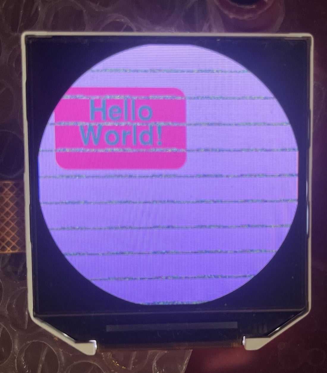
With filling the screen up with a pixel of the same color working, I rapidly got additional proof-of-concept work as shown in the video: squares of random greys at random pixel addresses. That was enough to prove to me that we can make a usable UI with SPI and Toit.
Goals Met?
All of this work was in pursuit of preventing Nest 2nd Gen thermostats from ending up in the landfill.
On October 25, 2025, Nest Thermostats of the 1st and 2nd generation will no longer be supported by Google. Nest and Google Home app access will stop working.
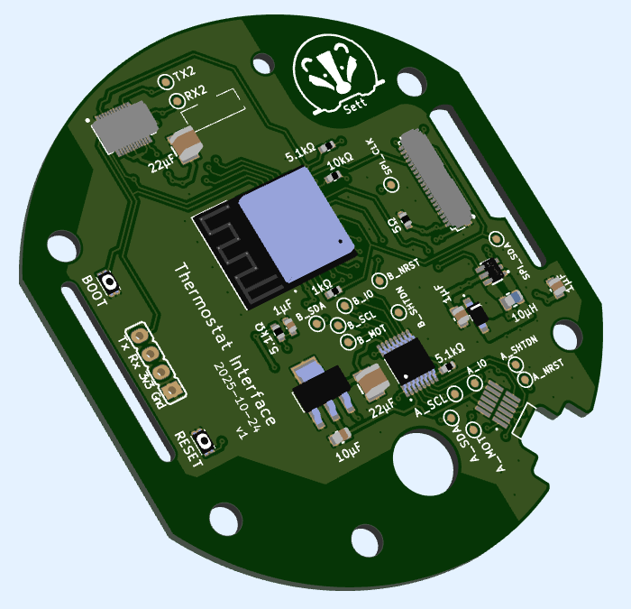
Sett is an open-source, enclosure-compatible version of the 2nd gen Nest thermostat. It reuses the enclosure, encoder ring, display, and mounts of the Nest but replaces the "thinking" part with open-source PCBs that interact with Home Assistant and other local-first home automation setups.
Pre-orders will be available soon - in the meantime, subscribe to support the project and get blog posts about development progress, like this one.